Showing posts with label Digital design. Show all posts

Saturday, August 1, 2015

Digital design of systolic array architecture for matrix multiplication

Systolic architecture consists of an array of processing elements, where data flows between neighboring elements, synchronously, from different directions. Processing element takes data from Top, Left and output the results to Right, Bottom.    
One of the key application of Systolic architecture is matrix multiplication. Here each processing element performs four operations, namely FETCH, MULTIPLICATION, SHIFT & ADDITION. As following figure depicts, "in_a", "in_b" are inputs to the processing element and "out_a", "out_b" are outputs to the processing element. "out_c" is to get the output result of each processing element.
Processing elements are arranged in the form of an array. In this case we analyze, multiplication of 3x3 matrices, which can be easily extended. Let say the two matrices are A and B. Following figure depicts how matrix A and B are fed into PE(processing element) array. 
Simulation of following matrices are as follows.
Verilog modules
module top(clk,reset,a1,a2,a3,b1,b2,b3,c1,c2,c3,c4,c5,c6,c7,c8,c9);

 parameter data_size=8;
 input wire clk,reset;
 input wire [data_size-1:0] a1,a2,a3,b1,b2,b3;
 output wire [2*data_size:0] c1,c2,c3,c4,c5,c6,c7,c8,c9;
 
 wire [data_size-1:0] a12,a23,a45,a56,a78,a89,b14,b25,b36,b47,b58,b69;
 
 pe pe1 (.clk(clk), .reset(reset), .in_a(a1), .in_b(b1), .out_a(a12), .out_b(b14), .out_c(c1));
 pe pe2 (.clk(clk), .reset(reset), .in_a(a12), .in_b(b2), .out_a(a23), .out_b(b25), .out_c(c2));
 pe pe3 (.clk(clk), .reset(reset), .in_a(a23), .in_b(b3), .out_a(), .out_b(b36), .out_c(c3));
 pe pe4 (.clk(clk), .reset(reset), .in_a(a2), .in_b(b14), .out_a(a45), .out_b(b47), .out_c(c4));
 pe pe5 (.clk(clk), .reset(reset), .in_a(a45), .in_b(b25), .out_a(a56), .out_b(b58), .out_c(c5));
 pe pe6 (.clk(clk), .reset(reset), .in_a(a56), .in_b(b36), .out_a(), .out_b(b69), .out_c(c6));
 pe pe7 (.clk(clk), .reset(reset), .in_a(a3), .in_b(b47), .out_a(a78), .out_b(), .out_c(c7));
 pe pe8 (.clk(clk), .reset(reset), .in_a(a78), .in_b(b58), .out_a(a89), .out_b(), .out_c(c8));
 pe pe9 (.clk(clk), .reset(reset), .in_a(a89), .in_b(b69), .out_a(), .out_b(), .out_c(c9));

endmodule

module pe(clk,reset,in_a,in_b,out_a,out_b,out_c);

 parameter data_size=8;
 input wire reset,clk;
 input wire [data_size-1:0] in_a,in_b;
 output reg [2*data_size:0] out_c;
 output reg [data_size-1:0] out_a,out_b;

 always @(posedge clk)begin
    if(reset) begin
      out_a=0;
      out_b=0;
      out_c=0;
    end
    else begin  
      out_c=out_c+in_a*in_b;
      out_a=in_a;
      out_b=in_b;
    end
 end
 
endmodule

Test-bench
module test;

 // Inputs
 reg clk;
 reg reset;
 reg [7:0] a1;
 reg [7:0] a2;
 reg [7:0] a3;
 reg [7:0] b1;
 reg [7:0] b2;
 reg [7:0] b3;

 // Outputs
 wire [16:0] c1;
 wire [16:0] c2;
 wire [16:0] c3;
 wire [16:0] c4;
 wire [16:0] c5;
 wire [16:0] c6;
 wire [16:0] c7;
 wire [16:0] c8;
 wire [16:0] c9;

 // Instantiate the Unit Under Test (UUT)
 top uut (
  .clk(clk), 
  .reset(reset), 
  .a1(a1), 
  .a2(a2), 
  .a3(a3), 
  .b1(b1), 
  .b2(b2), 
  .b3(b3), 
  .c1(c1), 
  .c2(c2), 
  .c3(c3), 
  .c4(c4), 
  .c5(c5), 
  .c6(c6), 
  .c7(c7), 
  .c8(c8), 
  .c9(c9)
 );

 initial begin
  // Initialize Inputs
  clk = 0;
  reset = 0;
  a1 = 0;
  a2 = 0;
  a3 = 0;
  b1 = 0;
  b2 = 0;
  b3 = 0;

  // Wait 100 ns for global reset to finish
  #5 reset = 1;
  #5 reset = 0;
  #5;  a1 = 1; a2 = 0; a3 = 0; b1 = 2; b2 = 0; b3 = 0;
  #10; a1 = 2; a2 = 4; a3 = 0; b1 = 4; b2 = 1; b3 = 0;
  #10; a1 = 3; a2 = 5; a3 = 7; b1 = 6; b2 = 5; b3 = 3;
  #10; a1 = 0; a2 = 6; a3 = 8; b1 = 0; b2 = 9; b3 = 7;
  #10; a1 = 0; a2 = 0; a3 = 9; b1 = 0; b2 = 0; b3 = 8;
  #10; a1 = 0; a2 = 0; a3 = 0; b1 = 0; b2 = 0; b3 = 0;
  #100;
  $stop;

 end
 
 initial begin
  forever #5 clk = ~clk;
 end
      
endmodule

Simulation results 
Output results can be seen after 6 clock periods from the time of data insertion. (time period between a1 gets 1 and the time of yellow marker). In usual case for 3x3 matrix multiplication altogether, it takes 3x3x3 = 27 times to do the iterations and calculations. But in this case it takes lesser time (x6 times), because systolic architecture is a class of parallel pipe-lined architecture. Here is the synthesis report and timing constraints of the RTL.


Target device - xc3s500e-4fg320
Tool used - Xilinx ISE 14.3
Now lets analyze the timing differences between above hardware design and the algorithm written in C++.

C++ 
#include<iostream>

using namespace std;

int main()
{
    int a[3][3] =
    {
        {1, 2, 3},
        {4, 5, 6},
        {7, 8, 9}
    };
    int b[3][3] =
    {
        {2, 1, 3},
        {4, 5, 7},
        {6, 9, 8}
    };
    int c[3][3];

    int sum;

    for(int i = 0; i < 3; i++)
    {
        for(int j = 0; j < 3; j++)
        {
            sum = 0;
            for(int k = 0; k < 3; k++)
            {
                sum += a[i][k] * b[k][j];
            }
            c[i][j] = sum;
        }
    }

    for(int i = 0; i < 3; i++)
    {
        for(int j = 0; j < 3; j++)
        {
            cout <<c[i][j]<<" ";
        }
        cout << endl;
    }
    return 0;
}
Output results

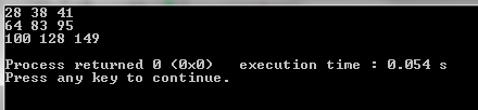
C++ execution time = 0.054s
Total delay of digital design = 7.765ns x 6 =   46.59ns 

Friday, March 20, 2015

Frequency Divider

A frequency divider, also called a clock divider or scaler or prescaler, is a circuit that takes an input signal of a frequency, fin, and generates an output signal of a frequency :

Source - Wikipedia

Where n is an integer (Wikipedia). In this post I explain how to implement the digital design of a simple clock divider(fin/2).

Source - ElectronicsTutorials


Verilog module
 module clock_divider (clk_in, enable,reset, clk_out);  
   input clk_in; // input clock  
   input reset;  
   input enable;  
   output clk_out; // output clock  
   
   wire  clk_in;  
   wire  enable;  
   
   reg clk_out;  
   
   always @ (posedge clk_in)  
     if (reset)  
       begin  
         clk_out <= 1'b0;  
       end  
     else if (enable)  
       begin  
         clk_out <= !clk_out ;  
       end  
   
 endmodule  
Test-bench
 module tb_clock_divider;  
   reg clk_in, reset,enable;  
   wire clk_out;  
     
   clock_divider U0 (  
    .clk_in (clk_in),  
    .enable(enable),  
    .reset (reset),  
    .clk_out (clk_out)  
   );  
     
   initial  
     begin  
       clk_in = 0;  
       reset = 0;  
       enable = 1;  
       #10 reset = 1;  
       #10 reset = 0;  
       #100 $finish;  
     end  
       
   always #5 clk_in = ~clk_in;  
     
 endmodule  
vivado simulation results
Simulation results
elaborated design
Elaborated design


Verilog simulation and RTL analysis was done in Vivado 2014.2. If you want to divide the input frequency further, (fin/4, fin/8, fin/16), you can extend the same circuit as follows.
 
Source - ElectronicsTutorials

Wednesday, January 7, 2015

Designing a BCD adder & subtractor with HDL

In computer based electronic items binary number system is used. But the human readable format is decimal number system. Binary coded decimal is a digital encoding mechanism to convert binary data between machine and human readable formats. To convert decimal data to binary, binary coded decimal adder subtractors are used in those electronic items. In this post I show you how to design a BCD adder subtractor using HDL (Hardware Descriptive Language) and here I use ‘Verilog’ language. Gate level design is the approach used to develop the BCD adder.

Here is the flow diagram of the circuit.

flow diagram of the circuit

Because the gate level design is used in this example the whole implementation is done using logic gates.

1-bit full adder

Here I start from the basic unit which is 1 -bit full adder. As shown in figure it has 3 inputs (A, B, Ci) and 2 outputs (S, Co). This circuit has designed using 2 XORs, 2 ANDs and 1 OR gate.


1-bit full adder
//define a 1bit fulladder
module fulladd(a, b, c_in,sum, c_out);
  input a, b, c_in;
  output sum, c_out;
  wire s1, c1, c2;
  xor (s1,a, b);
  and ( c1,a, b);
  xor (sum,s1, c_in);
  and (c2,s1, c_in);
  or (c_out,c2, c1);
endmodule
4-bit full adder

In the next step I combine 4 1 -bit full adders to create the 4-bit full adder as shown in figure. In this configuration it has 4bits per each input with a carry in has 4bit output with a carry out.


4-bit full adder
//define a 4-bit full adder
module fulladd4(a, b, c_in,sum, c_out);
  //i/o port declaration
  input [3:0] a, b;
  input c_in;
  output [3:0] sum;
  output c_out;
  //internal net
  wire c1, c2, c3;
  fulladd fa0(a[0], b[0], c_in, sum[0], c1);
  fulladd fa1(a[1], b[1], c1, sum[1], c2);
  fulladd fa2(a[2], b[2], c2, sum[2], c3);
  fulladd fa3(a[3], b[3], c3, sum[3], c_out);
endmodule

1-digit BCD adder


Here arithmetic operations are done using BCD number format. Hence the result of normal binary addition should convert to BCD format using error correction methods as shown in figure. For this configuration I use two 4-bit binary adders, 2 AND gates and 1 OR gate. In the error correction, 0110 binary 6 should add to the result of normal binary addition to convert the result in BCD format.
1-digit BCD adder
module bcd_adder( A, B, CIN, F, COUT);
  input [3:0] A, B;
  input CIN;
  output [3:0] F;
  output COUT;
  wire [3:0] Z,S;
  wire k,w1,w2,w3;
  fulladd4 add0(A, B, CIN, Z, k);
  and (w1,Z[3],Z[2]);
  and (w2,Z[3],Z[1]);
  or (COUT,k,w1,w2);
  assign S = {1'b0,COUT,COUT,1'b0};
  fulladd4 add1(Z, S, 0,F,w3);
endmodule

9’s compliment generator


Since the final circuit is made for both addition and subtraction operations, I'm going to make a special circuit with mode selection. 2’s compliment method is used for binary subtraction. But in BCD it must be 9’s compliment method. As shown in figure I have designed 9’s compliment generator in the following manner. 

9 - B = X 

truth table of 9's compliment generator
Here is the logic used in 9’s complement generator.
X3 = B3M’ + B3’B2’B1’M
X2 = B2M’ + (B2’B1 + B2B1’) M
X1 = B1
X0 = B0M’ + B0’M

9's compliment generator
module complement_generator(B, M, x);
  input [3:0]B;
  input M;
  output [3:0]x;
  wire w1,w2,w3,w4,w5,w6,w7,w8,w9;
  xor (x[0],B[0],M);
  assign x[1]=B[1];
  xor (w5,B[1],B[2]);
  and(w9,w5,M);
  not (w1,M);
  and (w6,B[2],w1);
  or (x[2],w9,w6);
  not (w2,B[1]);
  not (w3,B[2]);
  not (w4,B[3]);
  and (w8,M,w2,w3,w4);
  and (w7,B[3],w1);
  or (x[3],w8,w7);
endmodule

1-digit BCD adder subtractor


Combining the above 9’s compliment generator and the BCD adder it is able to design the 1 -digit BCD adder subtractor as follows.
 
1-digit BCD adder subtractor
module add_sub(A, B, CIN, M, F, COUT);
  input [3:0]A,B;
  input CIN,M;
  output [3:0]F;
  output COUT;
  wire [3:0]W;
  complement_generator comgen0(B,M,W);
  bcd_adder add0(A, W, CIN, F, COUT);
endmodule